Manufacturing Capability
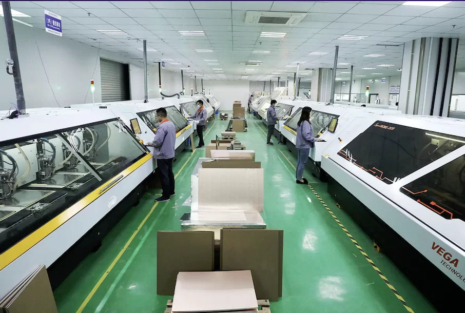
Cheerise Circuits operates 32,000㎡ of state-of-the-art production facilities with comprehensive PCB manufacturing capabilities. We continuously invest in the latest production and testing equipment to maintain our competitive edge. Our capabilities span from simple 1-2 layer boards to complex 38-layer prototypes, specialized materials, and complete PCBA assembly services.
Production Capacity
| Item | Mass Production | Sample |
| Max. Layers | 20layers | 38layers |
| Max. Board Size | 530*610mm | 550*1900mm |
| Material | CEM1,CEM3,FR-4,High Tg FR-4,Halogen free,High Frequency (Rogers,Arlon,Taconic,Nelco…), Aluminium base material, Copper base board material, Ceramic material board, etc | |
| Max. Board Thickness | 6.0mm | 8.0mm |
| Min. Core Thickness | 0.10mm | 0.075mm |
| Min. Track Width/Space | 3.5mil/3.5mil | 2.5mil/2.5mil |
| Max. Copper Thickness | Inner Layer: 10 Oz | Inner Layer: 20 Oz |
| Outer Layer: 10 Oz | Outer Layer: 40 Oz | |
| Min. Drill Size | 0.2mm | 0.15mm |
| Min. Laser Drill Size | 0.1mm | 0.076mm |
| PTH Diameter Tolerance | ±3mil | ±2mil |
| Aspect Ratio | 10:01 | 15:01 |
| PTH Wall Thickness | 18-25um | 16-35um |
| Min solder mask bridge | 0.10mm | 0.076mm |
| Min solder mask window | 0.10mm | 0.05mm |
| V-cutting Tolerance | ±0.10mm | ±0.10mm |
| Outline Dimension | ±0.10mm | ±0.10mm |
| Warp and Twist | ≤0.7% | ≤0.5% |
| Plating Hard Gold | 1.27um | 5.08um |
| Controlled Impedance | ±10% | ±5% |
| HDI Board | 1+N+1, 1+1+N+1+1 | 2+N+2, 3+N+3, ELIC HDI boards |
| Surface Treatment | HASL | HASL |
| HASL Lead Free | HASL Lead Free | |
| Immersion Gold | Immersion Gold | |
| Immersion Tin | Immersion Tin | |
| Immersion Silver | Immersion Silver | |
| ENEPIG (Electroless Nickel Electroless Palladium Immersion Gold) | ENEPIG (Electroless Nickel Electroless Palladium Immersion Gold) | |
| Flash Gold | Flash Gold | |
| OSP | OSP | |
| Gold Finger | Gold Finger | |
| Selective hard gold | Selective hard gold | |
| Item | Remarks and Testing | |
| Materials | Kapton, Polyimide, PET | FR4 for Rigid |
| Stiffener Materials | Polyimide, PET, FR4, SUS | |
| Flexible Board Layers | 1-4 Layers | Prototype 6 Layers |
| Rigid-Flex Board Layers | 2-10 Layers | Prototype 12 Layers |
| Max. Panel Size | 250mm*400mm | 250mm*30m, The whole roll production |
| Min.Track Width/Space | 0.051mm/0.076mm | 0.051mm/0.051mm |
| Min. Board Thickness | Single:0.1mm | 12.5um-50um(Flex)/0.1mm to 3.2mm(Rigid) |
| 2 layers:0.13mm | ||
| 4 layers:0.30mm | ||
| 6 layers:0.50mm | ||
| Min. Hole Size | Drill Hole: 0.20mm | 0.15mm for Prototype |
| Punching Hole:0.50mm | ||
| Aspect Ratio | 6:01 | 8:01 |
| Base Copper | 1/3Oz — 2Oz | 3 Oz for Prototype |
| Size Tolerance | Conductor Width:±10% | W ≤ 0.5mm |
| Hole Size: ±0.05mm | H ≤ 1.5mm | |
| Hole Registration: ±0.050mm | ||
| Outline Tolerance:±0.075mm | L ≤ 50mm | |
| Surface Treatment | ENIG | |
| OSP | ||
| Immersion Tin | ||
| Carbon Ink | ||
| Dielectric Strength | AC500V | |
| Solder Float | 288℃/10s | IPC Standard |
| Peeling Strength | 1.0kgf/cm | IPC-TM-650 |
| Flammability | 94V-0 | UL94V-0 |
| Item | Capability |
| Layers | 1-4 Layers |
| Metal core board type | Normal Aluminum pcb, COB MCPCB, Copper base board |
| Max. Board Size | 1900mm*480mm |
| Finished Product Thickness | 0.2-4.5mm |
| Min Trace& line spacing | 0.10mm |
| Warp & Twist: | 0.50% |
| Copper Thickness | 18-240 um |
| Hole Inner Copper Thickness | 18-40 um |
| Hole Position Tolerance | ±0.075 mm |
| Min Punching Hole Diameter | 1.0mm |
| Min Punching Square Slot Specification | 0.8mm*0.8mm |
| Silk Prints Circuit Tolerance | ±0.075 mm |
| Outline Tolerance | CNC:+/-0.1mm; Mould:+/- 0.75mm |
| Min Hole Size: | 0.2 mm (No limitation in Max hole dimention) |
| V-CUT Angle Deviation | ±0.5° |
| V-CUT Board Thickness Range | 0.6mm-3.2mm |
| Min Component Mark Character Style | 0.15 mm |
| Min Open Window for PADs | 0.1mm |
| Solder Mask | Green, White, Blue, Matte black, Red. |
| Surface Treatment | HASL and HASL Lead Free |
| Immersion Gold | |
| ENEPIG (Electroless Nickel Electroless Palladium Immersion Gold) | |
| OSP |
| Type | Capability | |
Material | AL203 ceramic (thickness in more than 2.0mm, need to be customized) | 0.25mm 114*114mm |
| 0.38mm 130*140mm | ||
| 0.5mm 130*140mm | ||
| 0.635mm 130*140mm | ||
| 0.8mm 130*109mm | ||
| 1.0mm 130*140mm | ||
| 1.2mm 130*109mm | ||
| 1.5mm 127*127mm | ||
| 2.0mm 130*140mm | ||
| Above is regular size,and other sizes can be customized, the maximum size we can do is 140*190mm | ||
ALN Ceramic (thickness in above 1.0mm, need to be customized) | 0.25mm 50.8*50.8mm | |
| 0.38mm 114*114mm | ||
| 0.5mm 114*114mm | ||
| 0.635mm 114*114mm | ||
| 1.0mm 114*114mm | ||
| Copper Pour | Type | High temperature fusion ceramic board(HTFC) Low temperature co fired multilayer ceramic board(LTCC) High temperature co fired multilayer ceramic board (HTCC) Direct bonding copper board (DBC) Direct plated Copper board (DPC) |
| Thermal Conductivity | AL203 Ceramic | AL2O3:20~51(W/mK) |
| ALN Ceramic | AIN:170~220(W/mK) | |
| Finished Copper Thickness | Copper thickness | 5um-1400um |
| Hole | Hole size | 0.05mm-30mm |
| Surface Finish | ROHS | ENIG、ENEPIG |
| Conductor | Characteristic | Pure silver route, pure gold route,Multi-metal overlay route |
| Min. Line width and spacing | Inner layers: | 20um/20um |
| External layers | 20um/20um | |
| Profiling | Maximum Board Dimension | 118*170mm/pcs |
| Layers | Sample | Mass production |
| Single Sided | 1~5 | 9~15 |
| Double Sided | 1~6 | 12~20 |
| 4 Layers | 3~8 | 15~25 |
| 6 Layers | 4~10 | 18~30 |
| 8 Layers | 5~12 | 20~35 |
| 10 Layers | 6~14 | 22~35 |
| Aluminum Base | 3~8 | 9~15 |
| 1L&2L FPC | 5~8 | 12~20 |
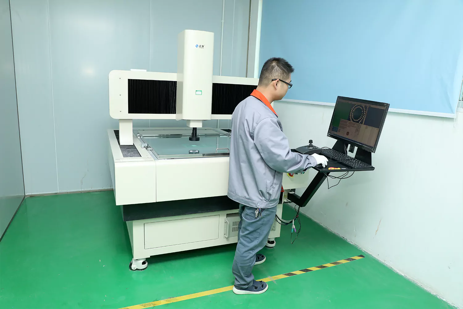
Quality Control System
Our commitment to quality is backed by certified management systems and comprehensive testing at every production stage:
– Material Incoming Inspection All raw materials are inspected and verified before production.
– In-Process Testing Every production step undergoes rigorous testing: drilling, plating, etching, and solder mask.
– Final Electrical Testing 100% electrical testing using flying probe or ICT.
– Visual Inspection AOI (Automated Optical Inspection) and manual visual checks.
– Certifications ISO 9001, ISO 14001, TS 16949, ISO 13485, ISO 45001 We continuously upgrade our production and testing equipment to maintain the highest quality standards.
quanlity control
Renowned for our expertise in PCB manufacturing, we excel in delivering high-quality, customized solutions to meet diverse industry needs. With cutting-edge technology and meticulous attention to detail, we ensure optimal performance and reliability.
15 Years Experience
Best Certification Team
Unlimited Revision
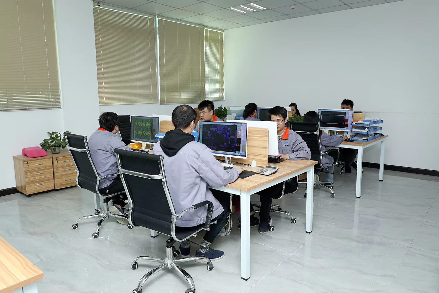
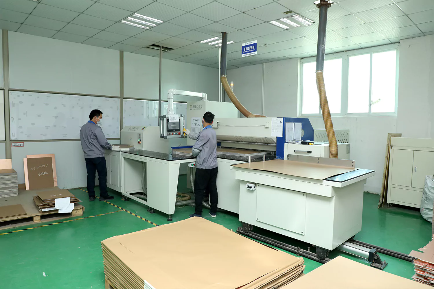
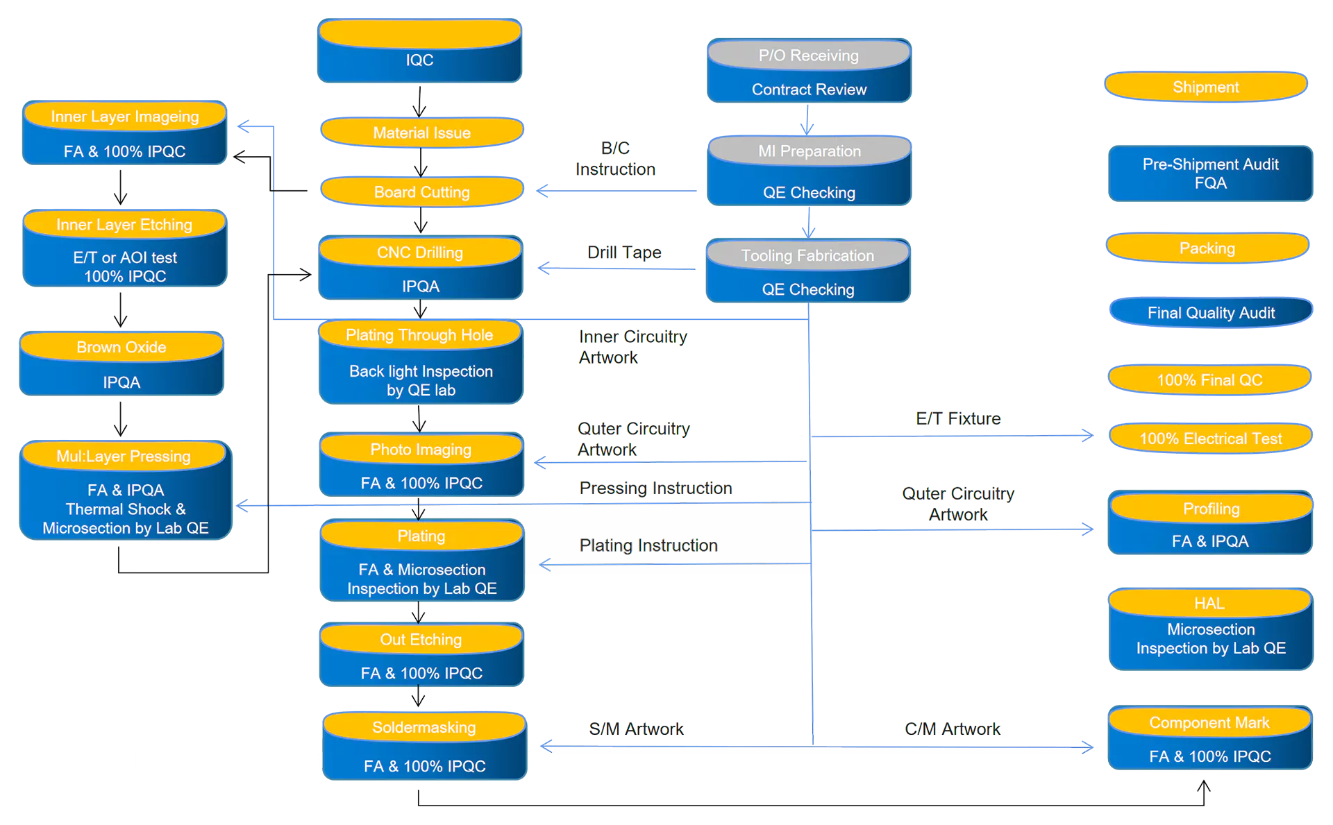
Production Process
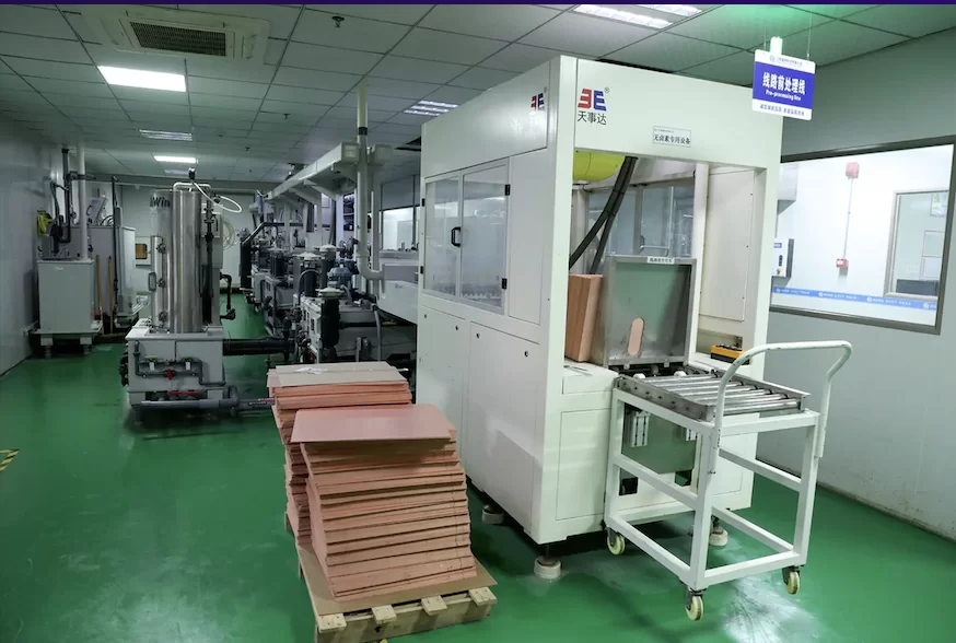
Key Equipments
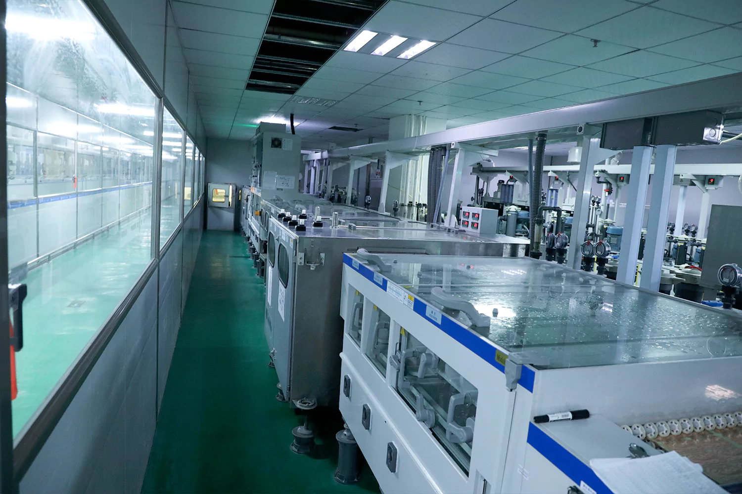
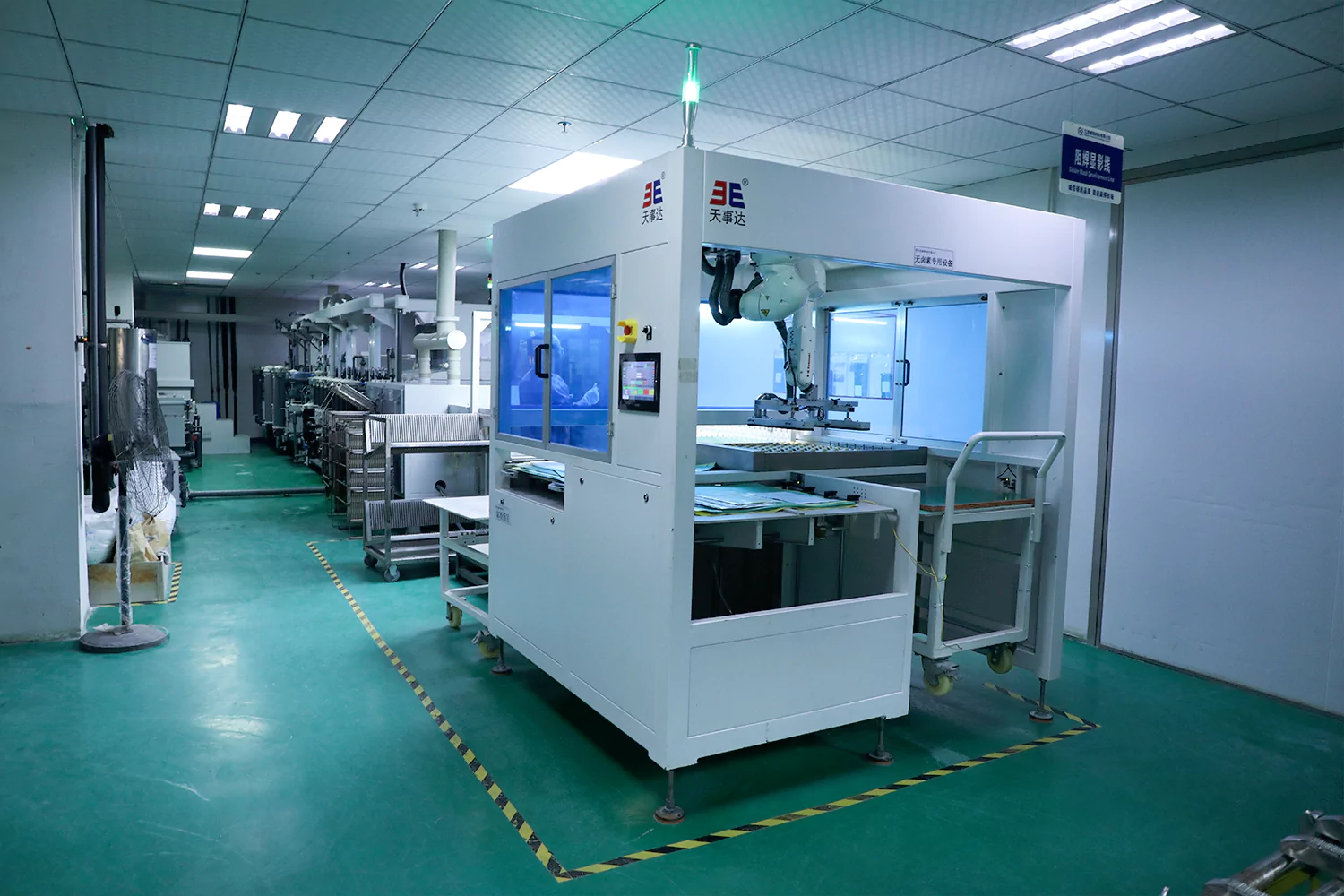
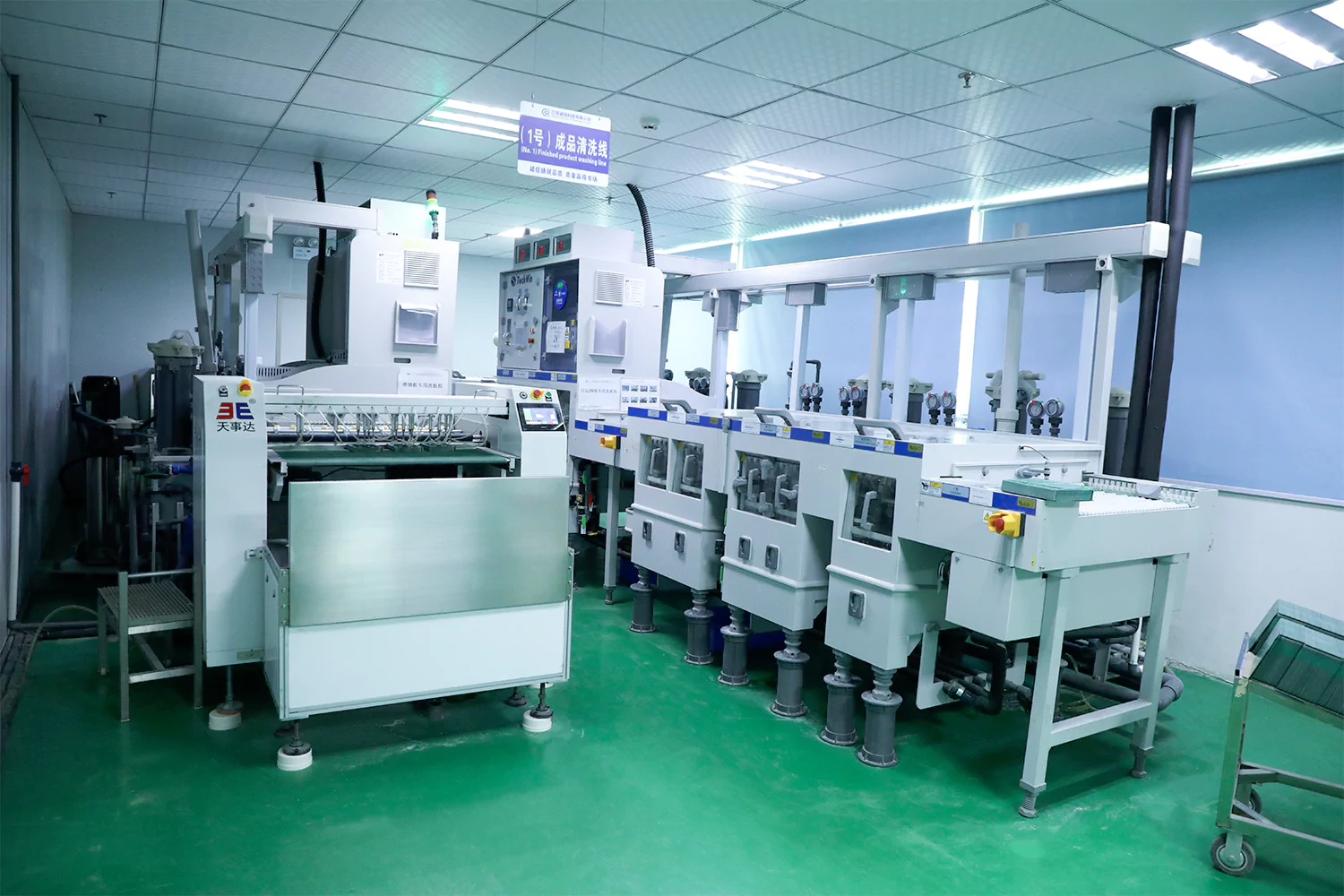
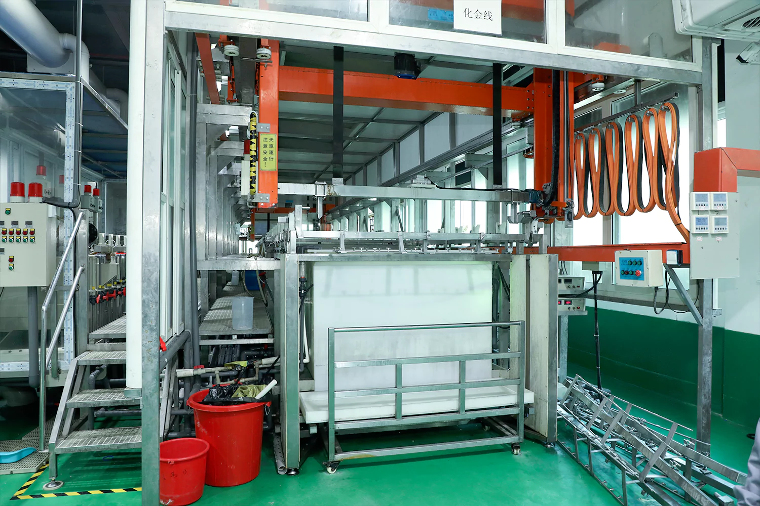
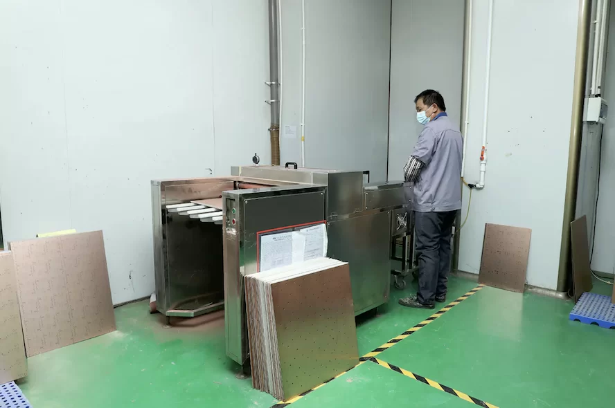
Factory tour