
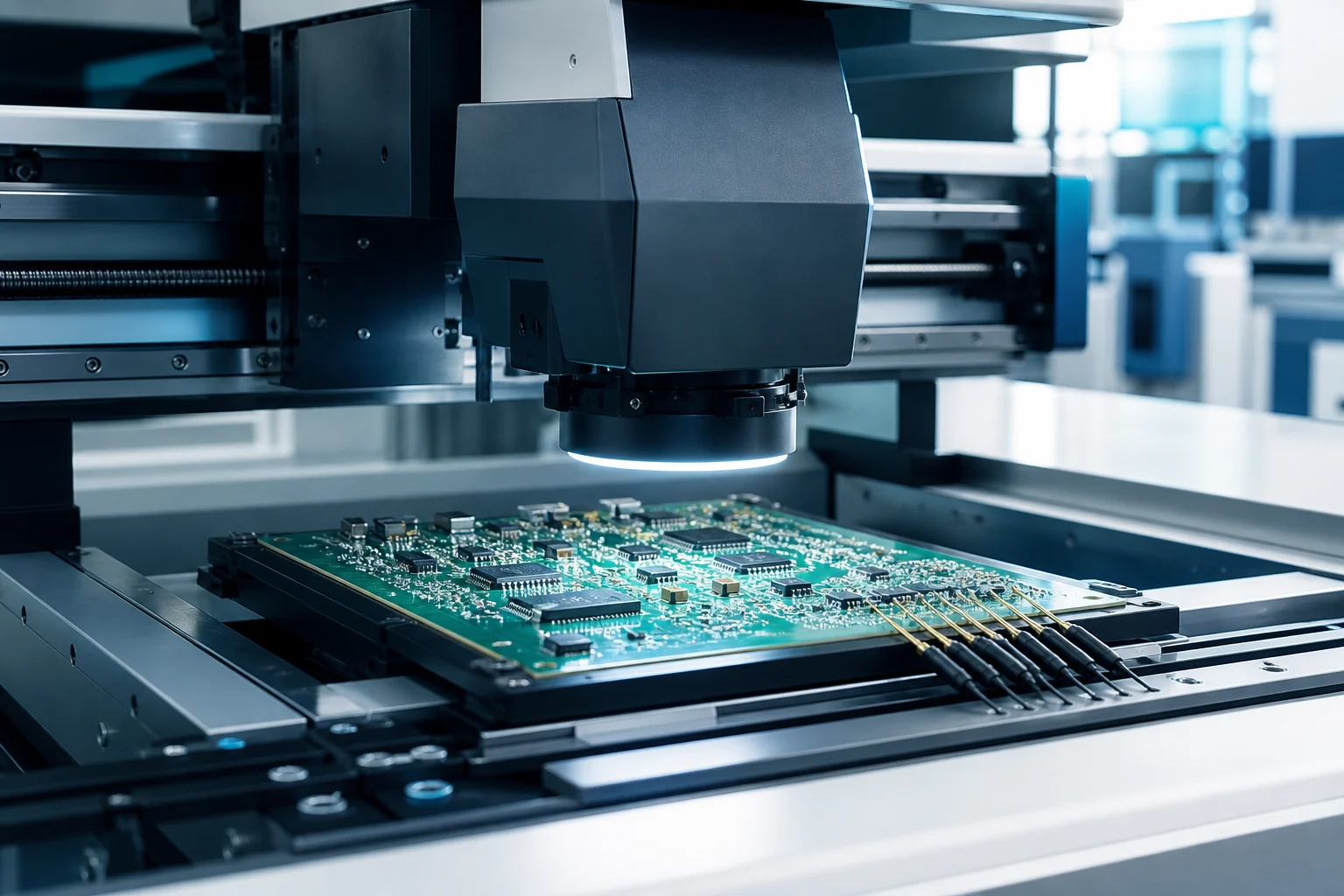
AOI, X-ray inspection, and flying probe testing are not interchangeable. Each method finds a different type of PCB or PCBA defect, so the right quality plan starts with one practical question: what failure are you trying to prevent?
For prototypes, industrial electronics, and complex assemblies, relying on a single inspection method can leave important risks uncovered. A board can pass AOI and still fail electrically. A board can pass X-ray and still need continuity or functional verification.
AOI: Best for Visible Assembly Defects
Automated optical inspection uses cameras and image comparison to inspect visible features on an assembled board. It is useful for detecting many surface-level assembly issues.
- Missing components
- Wrong polarity
- Component shift
- Solder bridges
- Tombstoning
- Obvious soldering defects
The limitation is straightforward: AOI can only inspect what it can see. Hidden solder joints under BGA, QFN, LGA, and other bottom-terminated components may need a different inspection method.
X-Ray Inspection: Best for Hidden Solder Joints
X-ray inspection helps reveal assembly defects that are hidden underneath components. This makes it valuable for boards with BGAs, QFNs, fine-pitch ICs, and dense component placement.
- BGA solder joint defects
- Voids
- Insufficient solder
- Internal bridges
- Hidden assembly issues under packages
X-ray inspection improves visibility into hidden solder joints, but it does not prove that every circuit net works as intended.
Flying Probe Testing: Best for Electrical Connectivity
Flying probe testing focuses on the electrical side of PCB quality. It can check nets directly without a dedicated fixture, which makes it especially useful for prototypes and lower-volume builds.
- Opens
- Shorts
- Incorrect nets
- Resistance and capacitance issues
- Certain placement-related electrical problems
Flying probe testing is not the same as functional testing. It helps verify connectivity and some electrical characteristics, but it does not fully simulate the end product’s operating conditions.
Comparison Table
| Method | Best For | Key Limitation |
|---|---|---|
| AOI | Visible component and solder defects | Cannot inspect hidden solder joints |
| X-ray | BGA, QFN, voids, hidden solder joints | Does not verify full electrical function |
| Flying probe | Opens, shorts, net continuity | Not a substitute for functional testing |
How to Choose the Right PCB Test Plan
The better question is not only “Was the PCB tested?” It is “Which failure modes were tested, and which risks remain?” A practical inspection plan may combine AOI, X-ray, flying probe testing, and functional testing depending on the board design and product risk.
Cheerise Circuits supports PCB fabrication and PCB assembly projects where inspection planning matters before production. Learn more on our Quality & Capability page or send your requirements through Contact Us.
FAQ
Can AOI catch all PCB assembly defects?
No. AOI is strong for visible defects, but hidden solder joints and electrical faults may require X-ray inspection, flying probe testing, or functional testing.
When should X-ray inspection be used?
X-ray inspection is useful when the PCB assembly includes BGAs, QFNs, LGAs, or other components with hidden solder joints.